Solid-State Quantum Transport Group
Tohoku University,
Graduate School of Science,
Department of Physics, Solid-State Quantum Transport Group
These are some of the key experimental equipment used in our laboratory.
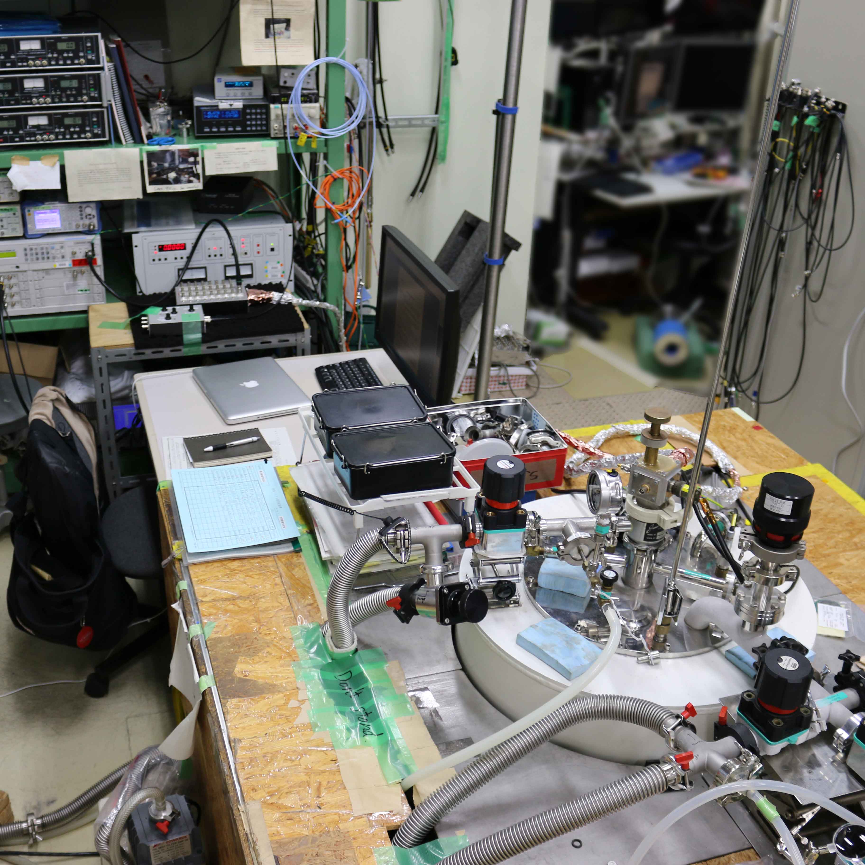
Low Temperature Measurements Lab
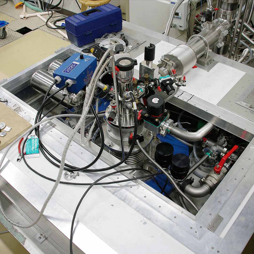
We use He-3/He-4 dilution refrigerators equipped with superconducting magnets in order to reduce thermal noise and measure behavior of solid state systems in the quantum regime. We have also introduced optical equipment into one of these refrigerators in order to perform low-temperature optical microscopy.
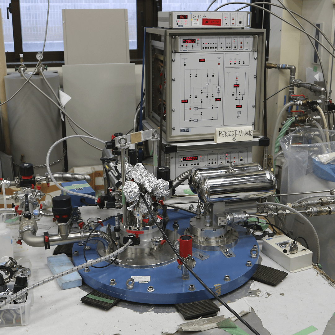
Dilution Refrigerator (in the low temperature measurements lab)
In our dilution refrigerators we can perform experiments at temperatures below 50 mK, and with superconducting magnets we can apply magnetic fields as high as 15 T.
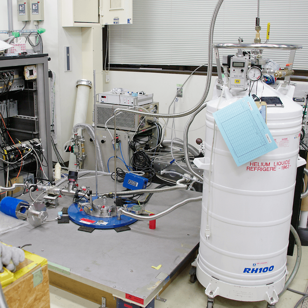
He-4 Refrigerator (in the low temperature measurements lab)
Our refrigerators utilizing He-4 can achieve temperatures over a wide range from room temperature to 1.5 K. Such temperature control is useful in comprehensive studies of magnetic transport phenomena.
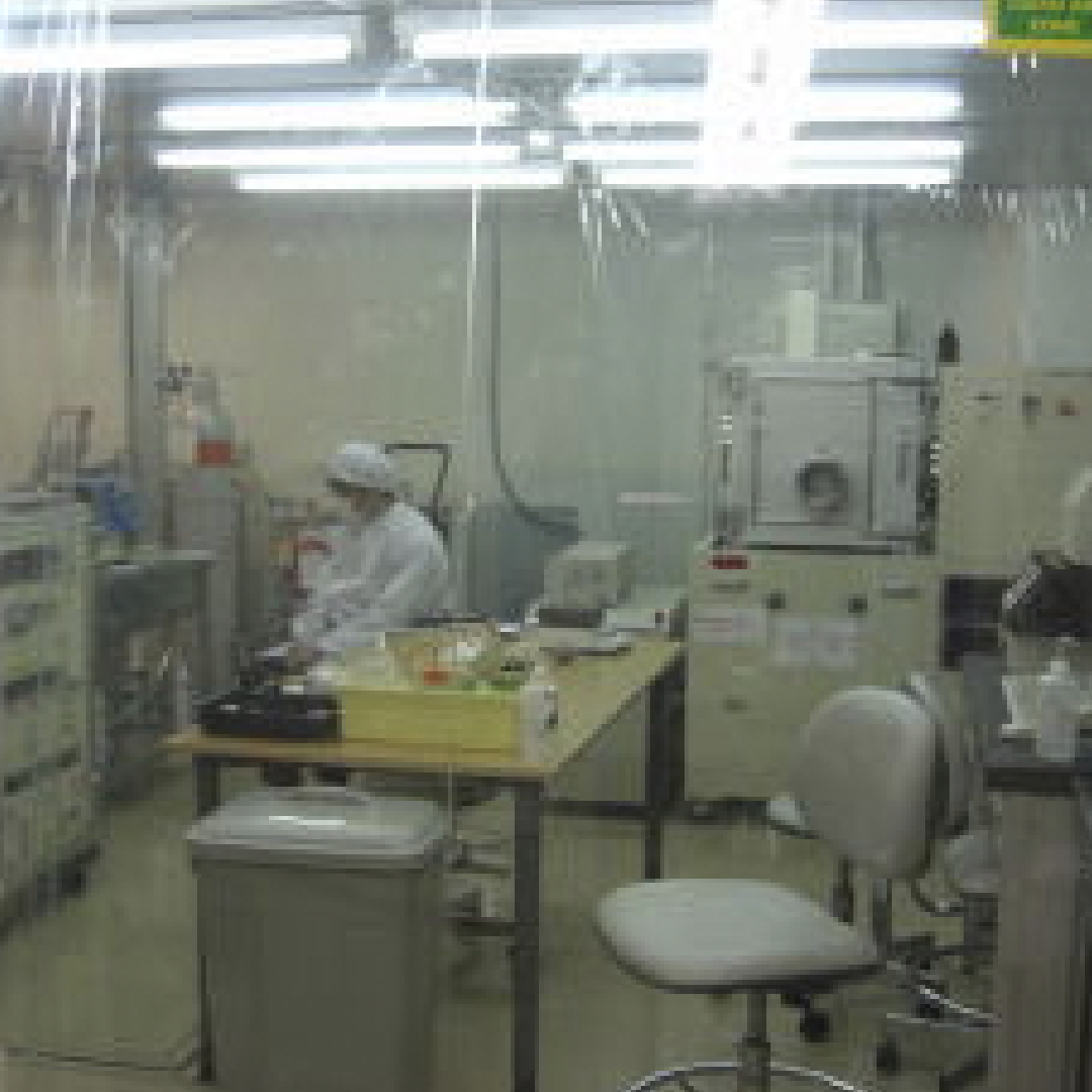
Sample Fabrication Cleanroom
Among the equipment in our clean booth we have an electron beam physical vapor deposition system, diamond thin-film depositor, rapid thermal annealing system, mask aligner and wire bonder, which we use to fabricate the semiconductor devices that we use in our experiments.
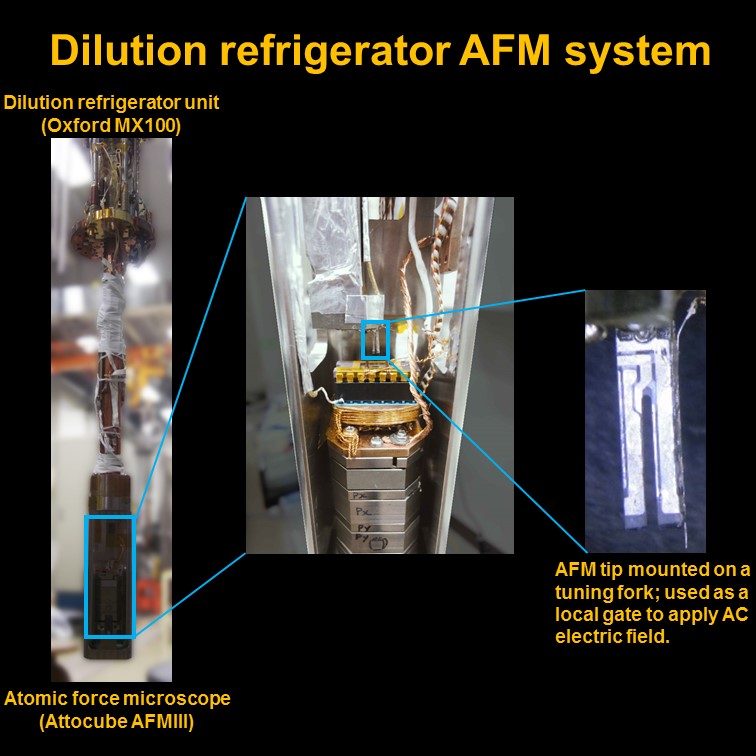
Ultra-Low Temperature, Ultra-High Magnetic Field Nanoprobe Apparatus
We are able to perform scanning tunneling microscopy (STM) and atomic force microscopy inside of a dilution refrigerator equipped with a superconducting magnet; this allows us to probe the behavior of electrons and nuclei within semiconductors at the nanoscale and under extreme conditions of temperature and magnetic field. We have successfully carried out STM at a temperature of 36 mK and field of 12 T.
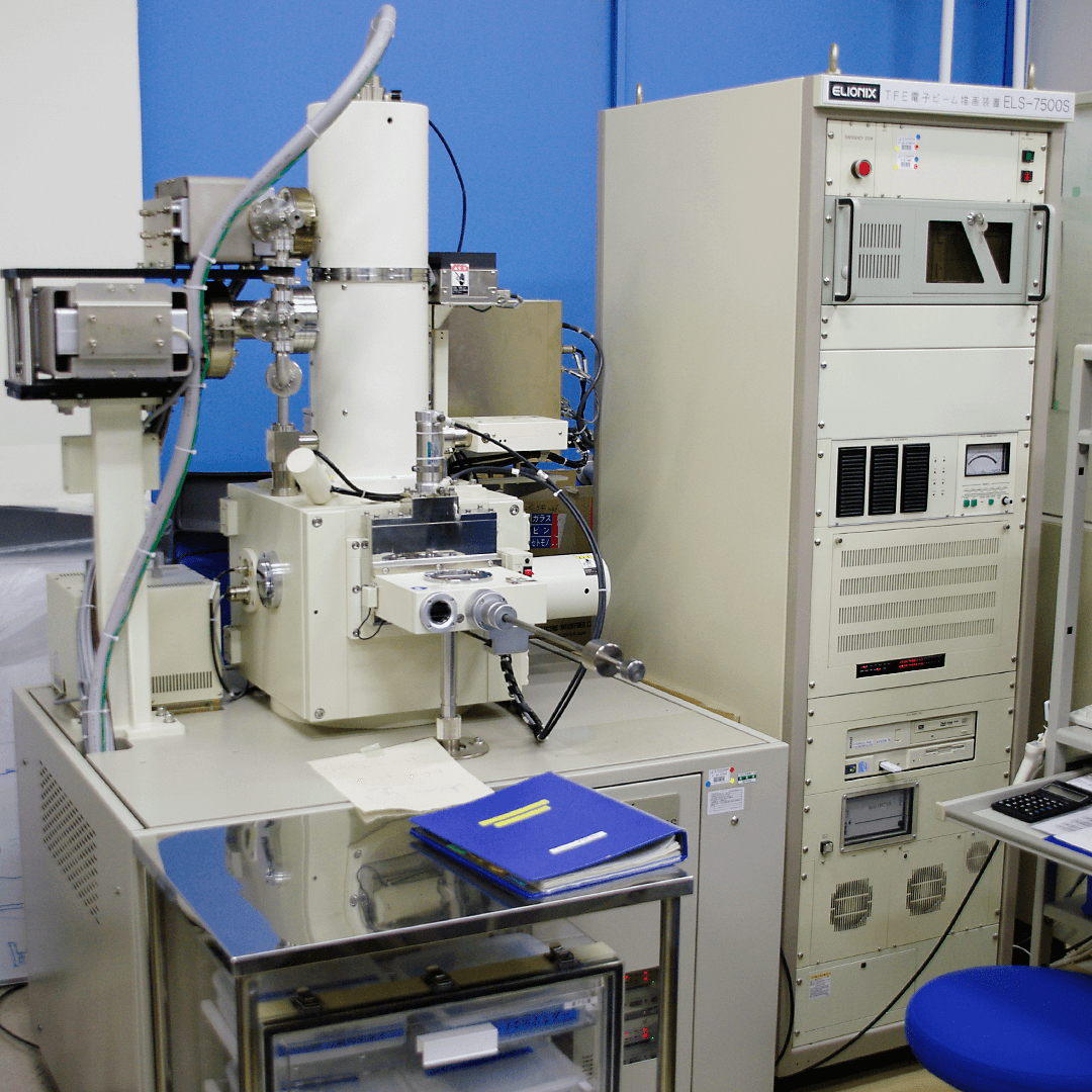
Electron-Beam Lithography System
This machine is owned by the ERATO project. Using a beam of electrons, it writes the nano-scale patterns which are implemented in our semiconductor devices. This way we can fabricate, test and utilize nano-devices that we have designed ourselves.